FPGA Composite NTSC Video
Table of Contents
This was originally published at https://github.com/agg23/fpga-compositevideo.
FPGA Composite NTSC Video
This project records an experiment I made to attempt to output composite video via a FPGA; direct driving IO pins and without any complicated hardware. This implementation supports up to 6 levels of greys, and only requires wires and 3 resistors to build the psuedo-DAC.
Getting Started
I started out on this project with a new devboard, the Tang Nano 9k. This gave me fast iteration times, and at least at the beginning, the joy of using a OSS toolchain. However, I quickly had to abandon the OSS toolchain due to lack of proper RAM support.
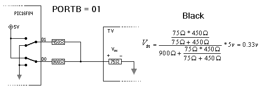
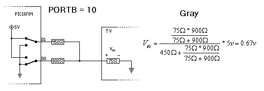
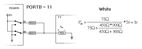
The general concept behind this project is creating a psuedo-DAC (digital to analog converter) using combinations of IO pins. Most projects that tried this used microcontrollers and two bits, which results in four total voltage values. NTSC requires a delta of 1V between the sync and brightest white levels, so naturally we target 0V-1V. Black then is placed at 0.3V.
The standard requires that TVs have an input impedience of 75 Ohms. Searching for a combination of resistors that can produce these target outputs (2 bit inputs, 3.3V driving voltage, 0.3V and 1.0V output) results in 450 Ohms and 900 Ohms. You can see a handy preview of the math below, stolen from the now dead Rickard Gunee website:
More on this math in a bit.
Now, if you wire up your circuit with two pins leading into each of the two resistors, with both of those tied to the positive pin of your RCA plug, theoretically you have everything you need to produce a NTSC video signal.
FPGA Implementation
In my initial implementation, I wanted to really understand the timing behind the NTSC signal, so I manually wrote my own timing code. Using the primary 27MHz clock of the Tang Nano 9k, I calculated the period of the clock, and determined the number of cycles needed in each of the sync signals. NTSC sync in black and white can be simplified down to:
- 4,700ns per horizontal sync. This encompasses almost all of the hblank period, but TVs accept it
- 58,856ns per vertical sync or pixel output. This results in a total line length of 4,700ns + 58,856ns = 63,556ns
- There are a total of 261 scanlines. One of those scanlines (I used 248, zero-indexed) output vsync, all others contain pixel data and hsync.
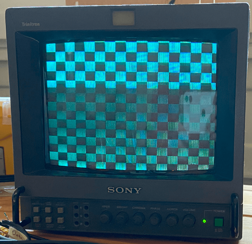
This can then be converted into a simple state machine that puts our two pins low when in sync, defaults to 900 Ohms being on (black), and varies between 900 Ohm, 450 Ohm (grey), and 900 + 450 Ohm (white). I used this to produce a checkered pattern.
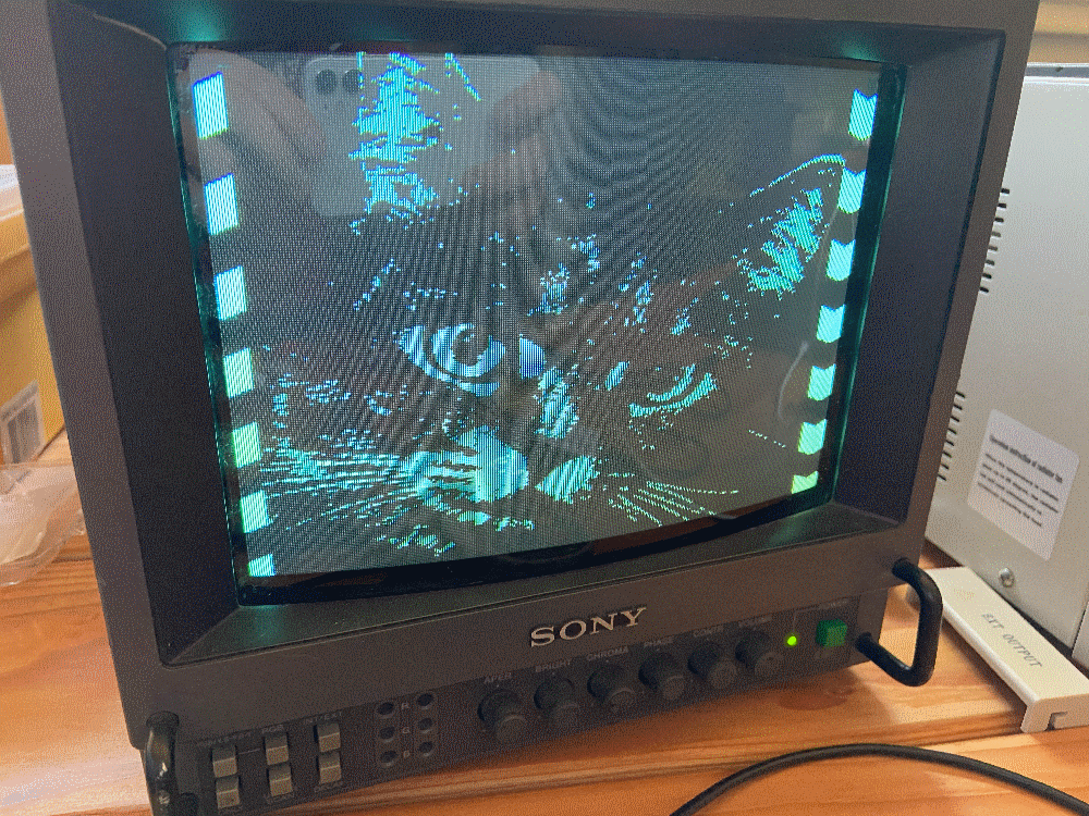
Following that, I went to display an image. After a long runaround trying to do things the right way (store greyscale image in Nano’s flash, read it out to PSRAM, render from PSRAM) and being blocked by bad tooling, bad support, and possibly flawed hardware, I gave up and went with the simple solution. There isn’t quite enough BRAM for a 256x240 (my target resolution) 8 bit image, so I scaled it to 4 bits, as we’re not going to have 256 colors anyway. With the image baked into the BRAM, I now just needed to maintain the XY counts for each pixel. Due to my familiarity with the system, I choose to use the NES’s system timings, matching exactly when the console would start/stop the sync pulses, as well as tracking what pixels are in overscan or not. This ended up being way simpler than the earlier method of tracking cycles absolutely (rather than per pixel).
This produced a nice image with surprising clarity. I chose my profile icon, not thinking about how dark it is (and thus not working well in black and white), but it seemed to turn out quite well.
Adding More Bits
As an extension of the projects I’d seen, I wanted to expand this system to 3 bits, and thus hopefully 7 colors. I very quickly realized that I didn’t really understand the math discussed above; calculating the resulting voltage from the system. After much deliberation and playing, I arrived at the following equations:
Let resistors be A, B, C, D (assuming 4 resistors)
Let A, B be pulled high, and C, D be pulled low
groundedPath = 1/(1/75 + 1/C + 1/D)

activePath = 1/(1/A + 1/B)

resultingVoltage = (groundedPath / (groundedPath + activePath)) * voltage
In other words:
- Resistors in series are added:
T = A + B + C - Resistors in parallel are the reciprocal of the reciprocals added:
1/T = 1/A + 1/B + 1/C - If a resistor is pulled low, it is in parallel with all other grounded resistors (all grounded resistors provide a separate path to ground, including the 75 Ohm TV impedience) (
groundedPath) - If a resistor is pulled high, it is in parallel with all of the other high resistors (
activePathadding reciprocals), and in series with the low resistors (groundedPath + activePath) - Dividing these two quantities and multiplying by our high voltage (3.3V) gets us our final voltage
With that math out of the way, how do we form a system of equations to solve for the optimal resistor values for us? After many iterations of looking at this, I realized it’s really not very easy and that I needed to approximate it the best I could. Some of the constraints looked like:
- We may not be able to hit the target voltages exactly (0.3V, 1.0V, everything in between), but we want to be as close as possible. Being too far away from 0.3V or 1.0V is super bad
- We may not be able to use all permutations of resistors. Maybe resistor A, C high, B low results in a voltage that’s out of range. We need to account for that
In the end I built a solution you can find in scripts/solver.ts. I’m sure it still has many problems, but it’s now good enough.
I configured it with the resistor values that I own and ran it, solving for 3 bits. It produced the output:
Best matches: [ 270, 330, 470 ]
Diff: 0.017571493125040277
None: 0
270: 0.5506745852430444
330: 0.4505519333806727
270, 330: 1.0012265186237168
470: 0.3163449745013234
270, 470: 0.8670195597443675
330, 470: 0.7668969078819959
270, 330, 470: 1.3175714931250402
This means our chosen resistor values are 270 Ohm, 330 Ohm, and 470 Ohm. The all high case results in 1.3V, so we can’t use that output, but we can use all of the others, giving us a total of 6 colors.
Splitting up our 4 bits of image data into 6 approximately equal sections resulted in a rather dark image, as many of these voltages are on the lower side of things. I tweaked the ranges to contain more lighter colors, and got the decently nice output you can see below:
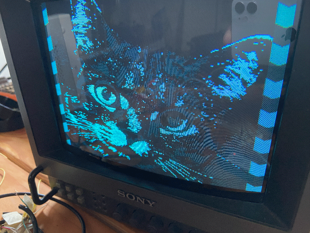
I noticed that my image seemed off-center, so I tweaked the counter numbers a bit. I found that adding 15 pixels to hsync resulted in a much better centering on both of my screens.
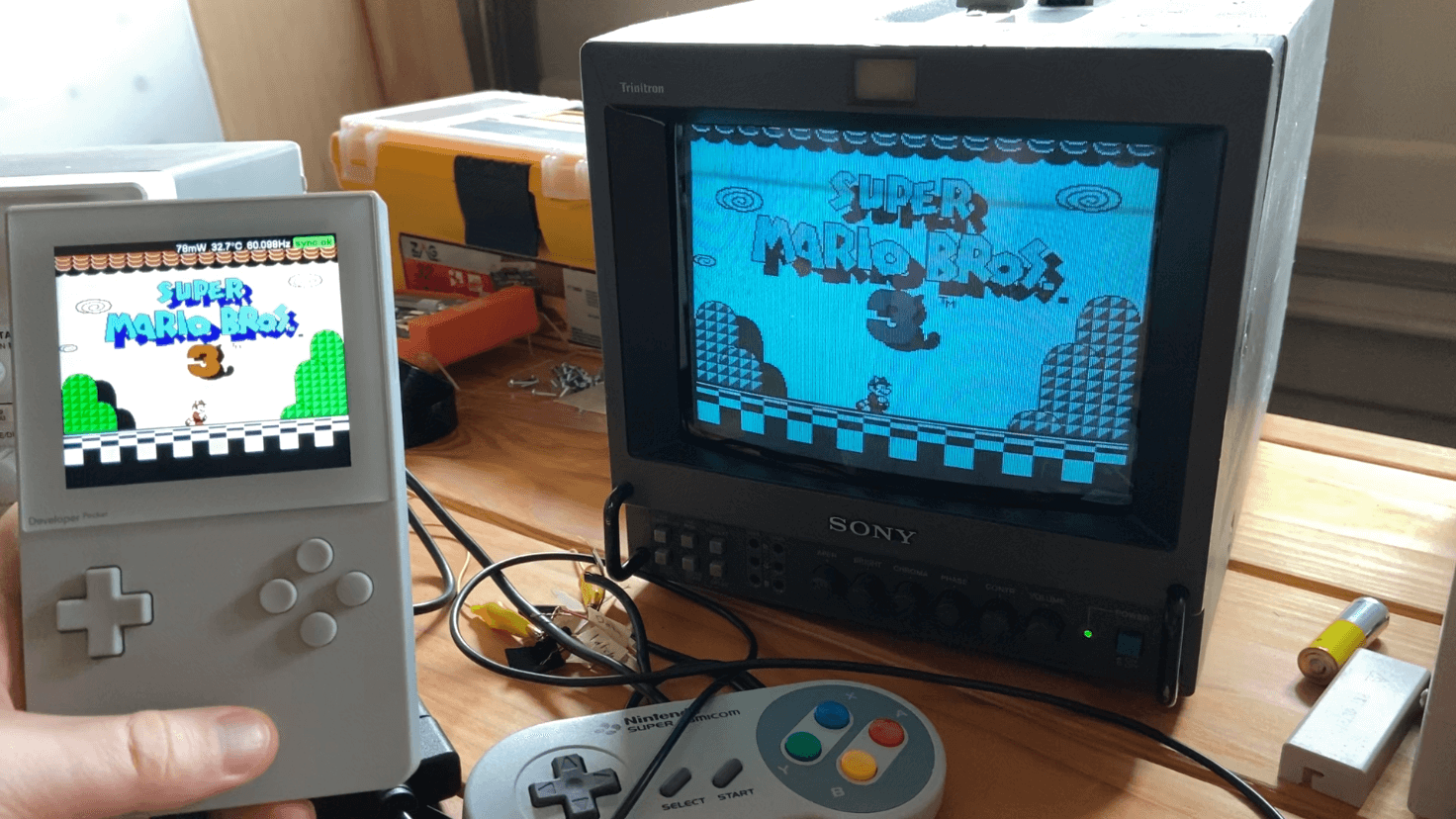
Video and Pocket Display
Satisfied with my colors, I was finally able to wire this project up to the Analogue Pocket. As expected, the static image worked perfectly straight out of the box, using the link cable as our IO pins. I then wired up the NES core to use the same rendering system to the link port, including the same values for converting the greyscale values to 6 colors. I had to introduce a RGB to greyscale converter (it’s not linear), but that was easy enough once I found an adequate example.
Hooking it all up produced the output I was hoping for; a surprisingly solid, good looking greyscale moving image of SMB on my CRT. I’m not going to be playing any games this way, but it’s still neat.